

The current energy crisis makes alternative sources of energy very attractive and research in these areas is a necessity. One of the most ubiquitous and abundant sources of energy is heat, and efficient thermo-electric devices are key to our ability to harvest thermal energy from many sources ranging from waste heat in power plants to geothermal and other sources. For this reason, simulation tools are well positioned to become the cornerstone of semiconductor material and device research and design, and have the potential for broad impact on a variety of uses and applications.
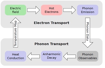
Improved thermal and thermo-electric simulation tools for devices and materials that are relevant to future advances in nanotechnology enable a detailed understanding of coupling between electron and phonon (charge and thermal) transport, their interdependence, and the impact on the performance of future nanoscale transistors, thermoelectric converters, and sensors.
Our research is currently organized around 5 themes:
R1. Nanostructured semiconductor thermoelectrics
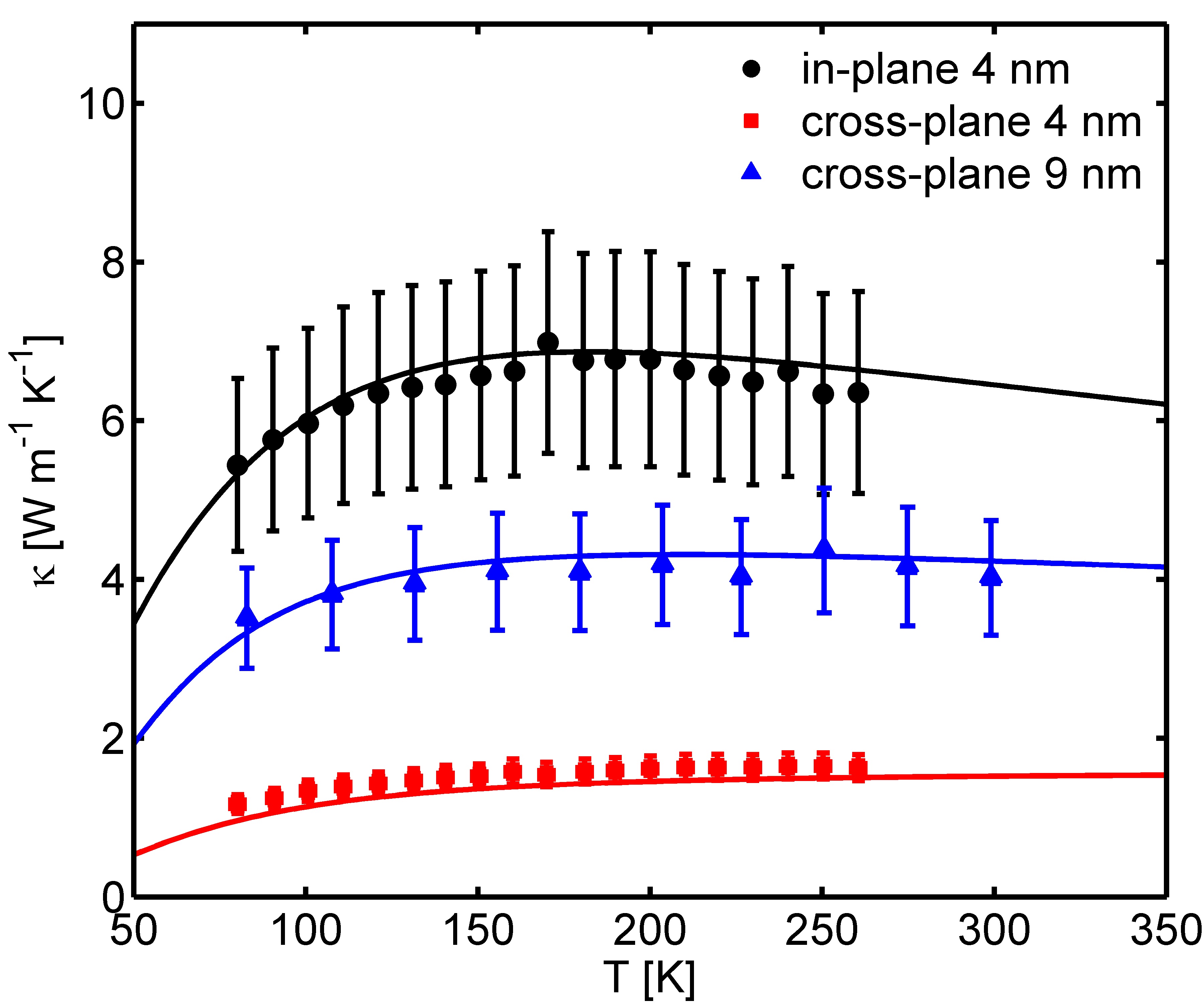
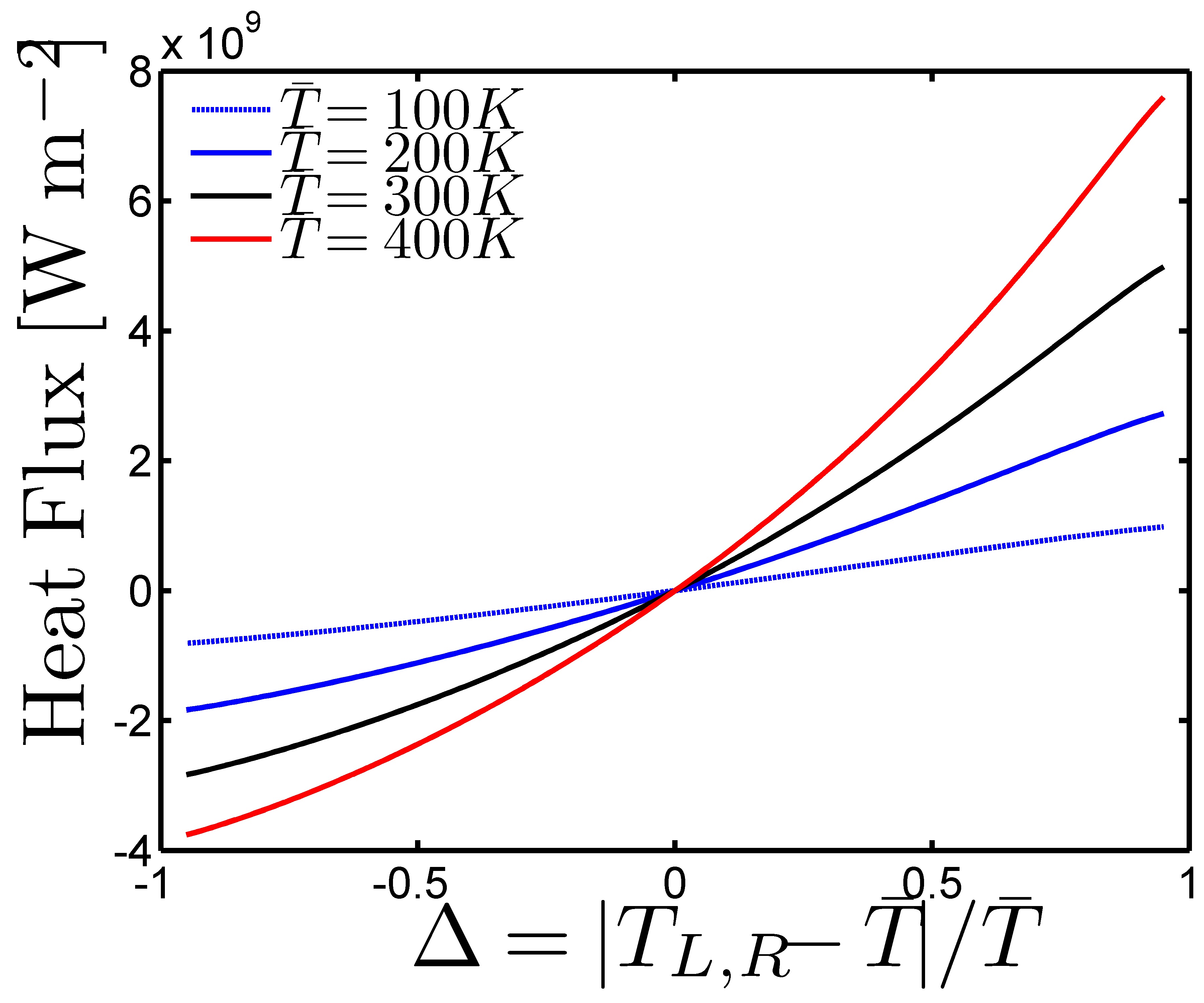
Nanoengineered silicon wires and nanocomposites have been shown experimentally to have tremendous potential as future thermoelectrics due to their high electrical and low thermal conductivity which, combined, yields a high figure-of-merit ZT, and consequently, very high energy conversion efficiency. Nonetheless, their usefulness hinges on our ability to simulate and predict which combination of material, geometry, and process is most efficient in energy harvesting applications. Past work in this area focused either on electrical or thermal conductivity calculations alone, but because of the strong interdependence of electrical and thermal transport, such decoupled approaches always fell short of a complete understanding of nanoscale thermoelectrics. Furthermore, far-from-equilibrium configurations like the non-linear Peltier effect are useful at low temperatures and in low-dimensional systems, but require advanced simulation that fundamentally couples together charge and thermal transport to capture the non-linear effects.
In order to reap the benefits of nanoengineered semiconductors for energy applications, we must understand the physics of charge dynamics, dissipation, and heat transfer at the nanoscale. Simulation tools I have developed contain the essential ingredients to unlock the physics of heat transfer in a multitude of complex nanostructures. I am developing numerical models to encompass a broader range of materials, including gallium nitride (GaN) and alloys such as silicon-germanium (SiGe). Such models will rely on coupling first-principles approaches with a full range of classical (Molecular Dynamics), semi-classical (Boltzmann transport and Monte Carlo), and quantum transport (Non-equilibrium Green’s functions) simulations. Non-linear effects will be captured by coupling together both charge and thermal transport in nanostructures.
R2. 2-D van der Waals heterostructures for energy applications
Monolayer graphene and graphene nanoribbons (GNRs) are taking center stage as the material of the future for sensor and high-frequency amplifier applications in nanoscale electronics. Graphene's strong carbon bonds lead to extremely high thermal conductivity, a property expected to be useful for thermal management in future densely-packed microelectronic circuits and chips. The key to the applicability of these novel ideas will be the thermal behavior of graphene, GNRs, and GNR-FETs and their performance gain over current technologies, especially when integrated with other materials. For example, electrical and especially thermal conductivity of graphene decreases dramatically when it is cut into nanoribbons , when interacting with other materials, such as a substrate. Large-scale CVD grown graphene samples are polycrystalline and contain numerous grain boundaries which further reduce electronic and thermal transport. Graphene-based metamaterials and plasmonics also hold promise for a wide range of future applications, ranging from solar cells to high-speed interconnects. In order to understand these issues, detailed transport simulation is a necessity, and developing tools that are capable of coupled electro-magnetic, electronic, and thermal transport simulation can have a key impact on the design of graphene devices, especially in the high-field, far-from-equilibrium regime.
R3. Nano-Phononic devices
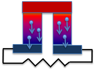
 Thermal diodes and thermal transistors, or "nanoscale heat valves", are geared toward controlling heat at the nanoscale level. They have been making the news recently as potential new candidates for a number of applications ranging from energy saving thermal insulation, all the way to thermal storage and computing in future microprocessors. Traditionally, we think of heat as a waste by-product of computation; yet if heat could be controlled and manipulated, it could be utilized for computing and storage, resulting in better energy efficiency. However, in order to design materials and devices based on precise nanoscale control of thermal transport properties, we need to be able to understand their interaction and predict their behavior at the nanoscale level. My work in anisotropic heat transfer in semiconductor nanomembranes demonstrated for the first time that boundaries in nanostructures induce a directional dependence of heat transfer. I will extend this idea to show thermal rectification in asymmetric nanoengineered semiconductors by building computational and theoretical models that enable a deeper understanding and lead to the design of novel nanoscale heat valves.
R4. Electro-thermal device simulation
 Self-consistently coupled electronic and thermal transport simulation of nanostructures is of large significance to the energy, integrated circuit, as well as the defense industry. Understanding thermoelectric and electro-thermal properties of semiconductors used in CMOS, high-frequency, optical, laser, and sensor devices, is crucial to future device design in many fields. One example is that of phase-change memory (PCM), which utilizes self-heating effects to switch nanostructured GST and GeTe between their crystalline and amorphous states.
My current work revolves around self-heating effects in nanoscale silicon MOSFETs through advanced coupled electro-thermal Monte Carlo simulation of complex device structures consisting of multiple materials, involving strained silicon, SiGe alloys, gallium-nitride (GaN) and graphene nanostructures, thereby strengthening the understanding of self-heating and dissipation in CMOS, QCLs, and sensor designs based on superlattices, nanowires, nanoribbons, and quantum dots.
R5. Computational Nanoscience on HPC and GPGPU platforms
Efficient numerical implementation of heat and charge transport dynamics requires the solution of coupled integro-differential transport equations to describe the physics of the problem at the nanoscale level. Such coupled multi-physics simulation offers a deeper understanding of the dynamics of heat dissipation and transport in nanostructures, but requires tremendous computational resources. General Purpose Graphical Processing Units (GPGPUs) can also be deployed to accelerate computation by utilizing the tremendous power of the graphical card available in every workstation. The inherently parallel tasks involved in electro-thermal transport simulation are a natural match to the GPU and heterogeneous MPI/GPGPU platforms. My work in porting simulation codes to the GPGPU platform demonstrated more than a ten-fold reduction in running time. I plan to expand the use of heterogeneous MPI/GPGPU computing in my research to tackle the challenge of coupled electro-magnetic and electro-thermal simulation at the nanoscale.